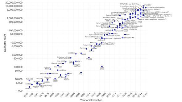
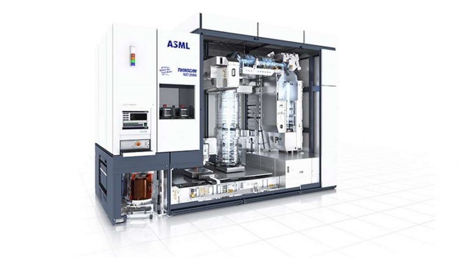
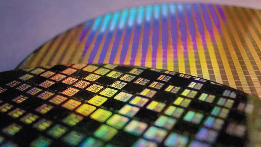
Moore’s Law states that the complexity for minimum component costs will increase twofold every two years – and for nearly 50 years, Intel co-founder Gordon Moore has been consistently right. It’s not been looking so rosy for this aged theory in recent years, however, and Intel’s own 10nm process has become a long drawn-out affair. But there may be another technology, with its own troubled history, that could finally be close to saving the day for this ageing law: Extreme Ultraviolet Lithography, or EUV.
EUV is a revolutionary new production process that will allow next-gen 7nm CPU production to offer higher yields, with lower complexity, and potentially lower costs too. It’s been the holy grail of chip manufacturers for years and is about to become a genuine reality.
It’s easy to dismiss the enormous and mind-boggling amount of work that goes into the best AMD and Intel processors. Those footnotes at the bottom of deep-dive product pages for your newly-purchased CPU or graphics card don’t often get due attention, but those little numbers – 14nm, 16nm, 22nm – represent the entire timeline for the age of computing. These fabrication process nodes have been chugging along in the minds of some very, very intelligent people for years, following the cadence of a law thought up in 1965: Moore’s law.
“Moore’s Law is fundamentally a law of economics,” former Intel CEO, Brian Krzanich, said in a company strategy statement, “and Intel will confidently continue to harness its value. The law says that we can shrink transistor dimensions by roughly 50% at a roughly fixed cost, thus driving twice the transistors for the same cost (or the same number of transistors for half the cost).”
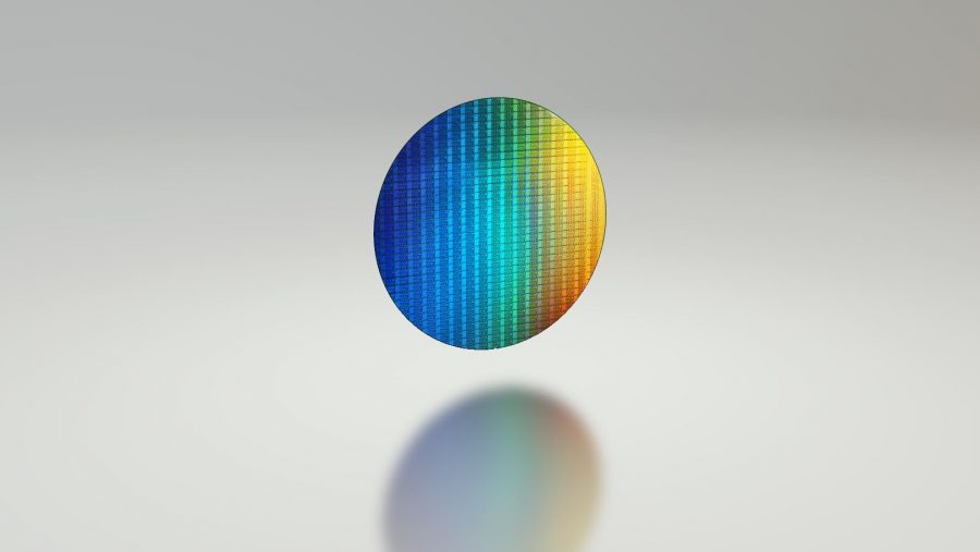
But that oversimplifies the rocky road it has taken to get your mass-produced PC componentry to the size it is today. Those billions of transistors, no matter the size – whether that’s 16nm for your Nvidia graphics card, 14nm for your Intel Coffee Lake CPU, 12nm for your AMD Ryzen 2 chip, or even 7nm for this year’s Zen 2 processors – all had to be whittled away with 193nm UV light, in a process aptly named 193nm immersion lithography. Why 193nm? Well, with shorter wavelengths it gets a little tricky past that point to use light that isn’t absorbed by the atmosphere itself (which EUV has to get around), or that causes unexpected behaviour.
Don’t panic, some particularly brainy humans already jumped the light wavelength hurdle by implementing lots of process steps, masking, multi-patterning, and clever optical tricks to get around the limitations at hand with 193nm immersion, but those have come with their own set of problems.
Top chips: Check out the best CPUs available today
The costs of denser chips will eventually outweigh the benefits on our current trajectory, and fresh process nodes are becoming less frequent as current fabrication techniques run out of steam – as evident by Intel’s recent delay of their 10nm architecture. Intel’s last CEO, Brian Krzanich, had already extended Intel’s trajectory during an earnings call in mid-2015, just about when Intel also threw the tick-tock cadence out of the window to combat a slowdown of process node progression.
“The last two technology transitions have signaled that our cadence today is closer to 2.5 years than two,” Krzanich says during the earnings call. “To address this cadence, in the second half of 2016 we plan to introduce a third 14nm product, codenamed Kaby Lake, built on the foundations of the Skylake microarchitecture but with key performance enhancements. Then, in the second half of 2017, we expect to launch our first 10nm product, codenamed Cannonlake.”
As made evident by the 14nm++ Intel Coffee Lake processors on the shelves today, it has since proven even more difficult than Krzanich had expected back in 2015 to continue process node development at a steady pace. Krzanich recently explained, in the company’s Q1 2018 earnings call, that the delays in 10nm products were due partially to “this being the last technology tied to not having EUV and the amount of multi-patterning and the effects of that on defects.”
Simply put: it’s just not worth making denser chips, and it’s getting increasingly difficult to do so. The steps required to manufacture chips have increased in quantity and complexity due to how gigantic the wavelengths of light are in comparison to the transistors they are outlining. Taking 193nm wavelengths down to 7nm requires a lot of clever trickery to work – GloFo CTO, Gary Patton, even went as far to call 7nm immersion lithography an “extreme sport” in an interview with IEEE Spectrum.
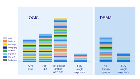
In turn, this increases time and money spent on every single product leaving a fab. Not only that, but the more complex a manufacturing process, the higher chance there is of something going wrong, and subsequently, the lower a fab’s yields will be. As you can imagine, that’s not too great when you plan on mass producing an entire CPU architecture for the immensely large computing market, and without angering shareholders.
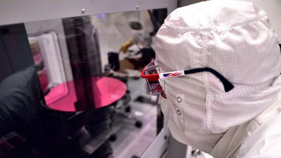
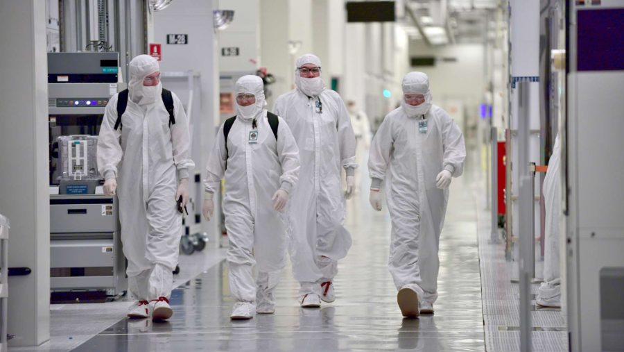
Luckily, EUV tech is ready to save the day. Theoretically, at least. It hasn’t quite got there yet, but we’ll get to that. The largest foundries, including TSMC, GlobalFoundries, Intel, and Samsung – supported by lead EUV proponent and fab manufacturer, ASML – are slowly but surely building up EUV fabrication units to maintain density competitiveness, and delay the fiscal cliff edge of constant node shrinks a little longer. As you might imagine, that is something Intel are particularly worried about for the road ahead due to their 10nm growing pains… sorry, shrinking pains. Intel don’t exist in a vacuum, however, and other fabs are sure to start running into evident trouble sooner or later.
So how does it work? In non-electrical engineering gibberish, EUV, or Extreme Ultraviolet, works by utilising a wavelength of only 13.5nm – that’s a massive step down from the 193nm light used to produce computer chips today. That means fabs can reduce the optical trickery required to shrink chip designs down to size, removing some multi-patterning steps along the way and, ideally, save money, time, and increase yields. ASML believe future 7nm immersion lithographies will require 34 steps, while 7nm using EUV will require only nine.
So is EUV the future of all chip fab floors? Yes and no.
We still haven’t had totally EUV chips in our gaming PC for a few reasons, and they’ve kept EUV adoption on a leash for some time. First up, one thing that EUV struggles with is power. It requires a 250-watt EUV source currently unavailable en masse. Without a powerful enough source, EUV can’t meet the production goals required of it to make fiscal sense – although they are close to being field ready as we speak. The delays in getting EUV ready for mass production have caused many large fabs, such as TSMC and GloFo, to rely on traditional methods for their 7nm processes – a process node previously touted as the one where EUV will shine.
Secondly, EUV may require a pellicle. These are thin membranes that cover the photomask (the template that outlines the CPU design for manufacturing) during production, and protect any unwanted particles from destroying the ‘printed’ design onto the silicon. If an EUV fab was running at full whack, a single dust particle could affect 125 silicon wafers every hour, and potentially even more as the tech improves.
Making sure the pellicles don’t break is another worry for foundries looking to adopt the lithography, and more robust pellicles are proving tough to manufacture. At least for logic fabrication, CPUs and GPUs for example, pellicles may well be necessary. Fabs could ditch the pellicle if need be, but that requires some serious clean-room protocols. Luckily, for memory production, which conveniently features some redundancy and also requires less photomask changes, a costly pellicle may not be essential.
Similarly, EUV also requires a vacuum to function so that the EUV light particles aren’t absorbed by air itself – but that’s not quite so difficult to attain.
It’s not all bad for the future of EUV, however. As TSMC has outlined, its future plans are to utilise EUV across its 7nm node. AMD’s future CPUs and graphics cards will therefore be using EUV potentially as soon as the Zen 3 CPU architecture, and while Navi may be a little bit hopeful, the GCN-agnostic architecture potentially incoming post-Navi could utilise the EUV tech. All AMD’s roadmaps eventually lead to EUV. TSMC has also confirmed a 5nm process node on EUV sometime in 2019.
Samsung has supposedly invested the most heavily in EUV, and there have been rumours of Intel’s high adoption rate, too – supposedly committing a high volume of funds toward the emerging tech for a 7nm EUV node in 2020. Intel has maintained that its transistors are denser than everyone else’s, but EUV could level out the playing field somewhat – regardless of who’s denser than who.
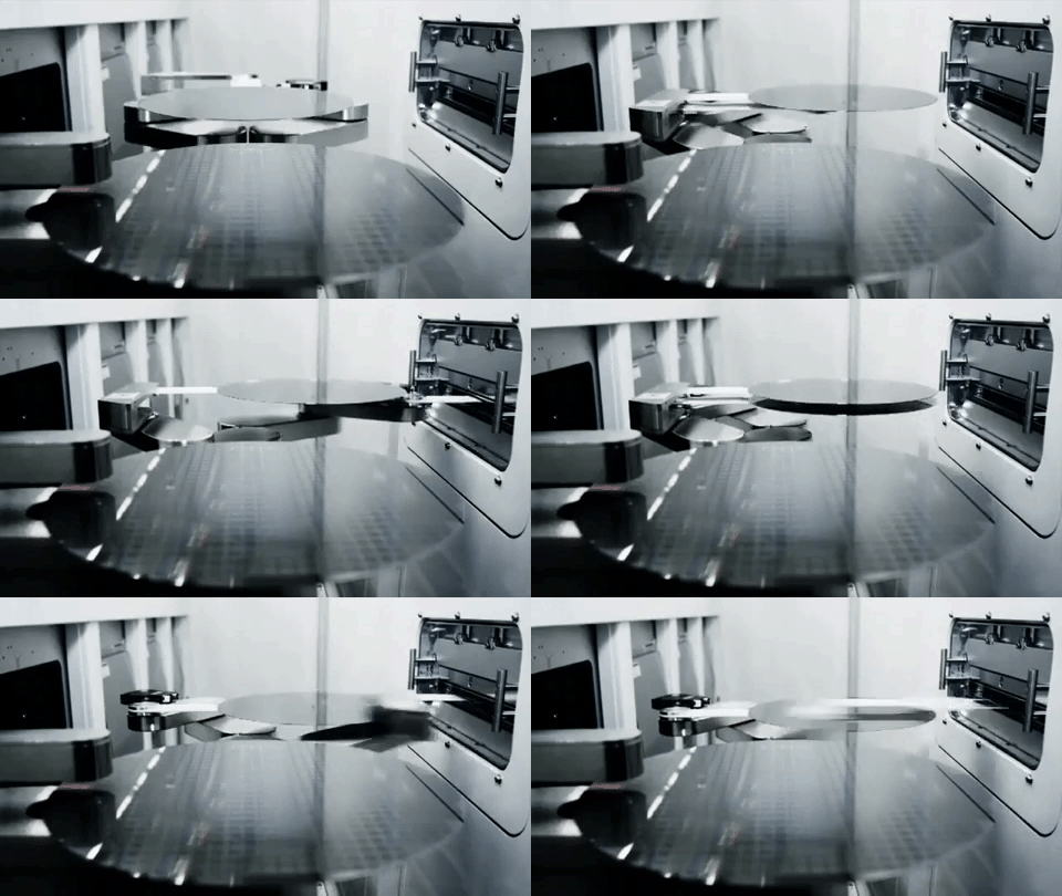
With ASML working on upping productivity levels for EUV and solving some of these crucial hurdles to mass production, rollout and implementation of EUV in fabs is expected to grow throughout the remainder of 2018, with ASML expected to double shipments in 2018, and start reaching full-scale manufacturing in 2019.
But the real question is whether EUV be any cheaper for us ordinary folk? At first, the real cost benefit from EUV is likely only going to affect semiconductor manufacturers’ bottom lines. These new EUV fabs don’t come cheap, in fact they cost $119 million a pop, and silicon prices are expected to rise by 20% in 2018 alone. Ouch, that’s Moore’s second, and lesser known, law coming into play. Unfortunately, the real booming chip market of Internet of Things SoCs and ASIC chips will likely benefit most from rapid-fire and cheap chip production more than power-hungry processors for us enthusiasts.
But, as the tech matures, yield rates will go up, and manufacturing time and costs will drop, potentially causing a knock-on effect of cheaper chips for gamers within the wider processor market.
That is, so long as another approach doesn’t render the transistor density conundrum invalid first. That’s where 3D device architectures enter the scene. We recently heard TSMC speak about their own silicon stacking tech, WoW (that’s the name, but I am also genuinely impressed), potentially allowing multiple packages to occupy a single package-sized footprint through the use of TSVs (through-silicon vias). But they aren’t the only ones to apply liberal chip stacking to solve the density issue – flash memory has been utilising this technique for years, and there’s also Intel’s own heterogeneous EMIB (Embedded multi-die interconnect bridge) tech for mixing and matching entirely different chips and processes.
Moore even talked about the potential for larger chips to be built up from smaller components and ‘interconnected’ back in his original 1965 paper, allowing manufacturers to “construct a variety of equipment both rapidly and economically.” Now, that’s foresight.
So maybe EUV will help save Moore’s Law for just a little longer, ideally ushering in an age where semiconductor chips are cheaper than ever. It seems more likely, however, that EUV will work in tandem with current immersion tech for the time being, and coincide with further 3D logic chip stacking development to pack as many transistors as possible under one roof.
If only, at least, until quantum computing reaches mass production and turns classical computers into a relic of a rudimentary past.
