Table of Contents
IPC-4761 Via Protection: Via Tenting, Via Plugging, Via Filling
Several technical or production-related demands for PCB manufacturing require via protection. These types of via covering are possible:
- Simply Covering: Via Tenting or Tented Vias
- Partially Filled: Via Plugging or Plugged Vias
- Completely Filled: Via Filling or Filled Vias
In the following, you will find a comparison of the technical capabilities of via covering protection. The reference is the IPC-4761 [Design Guide for Protection of Printed Board Via Structures]. The following chart is a summary of the different types of via plugs called out in this document, which reflects the IPC effort to standardize the via covering protection process:
| Type | Description | Via Covering Material |
|
I-a I-b |
Tented Via (one-sided)
Tented Via (double-sided) |
Dry film solder mask |
|
II-a II-b |
Tented & Covered Vias (one-sided)
Tented & Covered Vias (double-sided) |
Dry film solder mask + LPI solder mask |
|
III-a III-b |
Plugged Via (one-sided)
Plugged Via (double-sided) |
Plugging Epoxy (non-conductive paste) |
|
IV-a IV-b |
Plugged & Covered Via (one-sided)
Plugged & Covered Via (double-sided) |
Plugging Epoxy + LPI solder mask |
| V | Filled Via | Plugging Epoxy (non-conductive paste) |
|
VI-a VI-b |
Filled & Covered Via (one-sided)
Filled & Covered Via (double-sided) |
Plugging Epoxy + LPI solder mask |
| VII | Filled & Capped Via | Special Plugging Epoxy + Copper Plating to planarization. |
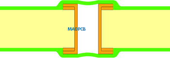
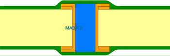
Via Tenting
IPC-4761 Type I: Tented Via
Dry film solder mask is stretched over the Via. No other materials are added.
One-sided: Type I-a

via protection
Double-sided: Type I-b
via protection
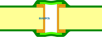
IPC-4762 Type II: Tented & Covered Via
The via is completely covered with dry film solder mask and overprinted with normal solder mask, afterwards.
One-sided: Type II-a

Double-sided: Type II-b
Application
- Protect of solder paste floating up to the component side
- Enables vacuum-adaption for production
- Covering of critical vias, e.g. beneath BGA
Alternatives
You can apply Via Filling, alternatively in via protection.
Through cutting the solder mask clearance, you can ensure a sufficient solder mask bridge for BGAs. Using this method, the via annular rings will be partly covered with solder mask.
Parameters
| Covering | Max. Drill Diameter |
| Via Tenting | 0.3mm |
Designation
It is sufficient to cover the vias within the solder mask layer.
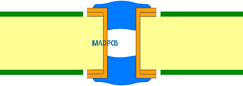
Via Plugging
IPC-4761 Type III: Plugged Via
The via is partially filled with non-conductive paste.
One-sided: Type III-a

Double-sided: Type III-b
IPC-4761 Type IV: Plugged & Covered Via
The via is partially filled with non-conductive paste and overprinted with normal solder mask, afterwards.
One-sided: Type IV-a

Double-sided: Type IV-b
Multi-layer PCB recommends one-sided plugging (Type III-a / Type IV-a) as there is a chance of cracks through encapsulated gas while soldering double-sided plugged vias..
Application
- Protection of solder paste floating up to the component side.
- Enables vacuum-adaption for production.
Parameters
| Covering | Min Drill Diameter | Max Drill Diameter |
| Via Filling | 0.25mm | 0.5mm |
Designation
Copy the vias to be filled into an additional layer and define that layer with your PCB fabrication notes.
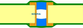
Via Filling
IPC-4761 Type V: Filled Via
The via is filled completely with non-conductive paste.

via protection
IPC-4761 Type VI: Filled & Covered Via
The via is filled completely with non-conductive paste and overprinted with normal solder mask, afterwards
One-sided: Type VI-a

via protection
Double-sided: Type VI-b
IPC-4761 Type VII: Filled & Capped Via
The via is plated-through and cleaned -afterwards a non-conductive paste is forced in and hardened -the ends are planarized, metallized and plated-over. Hence, the surface is planar and solderable.

Via Filled and Capped Technology is mostly used for Via-in-Pad (VIP) solutions and is also applied for stacked and staggered via & microvia in HDI boards. Via plugging facilitates routing of additional conductor traces between BGA vias amongst other things.
Filled & Capped Vias are also possible for Blind Vias.
Application
- Space saving
- Protection of solder floating up to the component side.
- Protection of solder floating up to the component side.
- Facilitates stacked and staggered Microvia for sequential build-up (SBU) multilayers.
- Facilitates Via-in-Pad Technology, e.g. for BGAs.
Parameters
| Covering | Min Drill Dia. | >Pad Dia. | Max Drill Dia. | >Pad Dia. | Aspect Ratio |
| Filled & Capped
IPC-4761 Type VII |
0.15mm | 0.35mm | 0.4mm | 0.6mm | 1:12 |
| Filled & Capped
eletroplated |
0.1mm | 0.3mm | – | – | 1:10 |
*Filled & Capped Vias blind vias have an aspect ratio of 1:1.
Designation
Copy the vias to be plugged into an additional layer and define that layer with your solder paste.
MADPCB strongly recommends that all vias be tented, filled and/or capped, especially under BGA packages according to IPC-4761 covering protection.