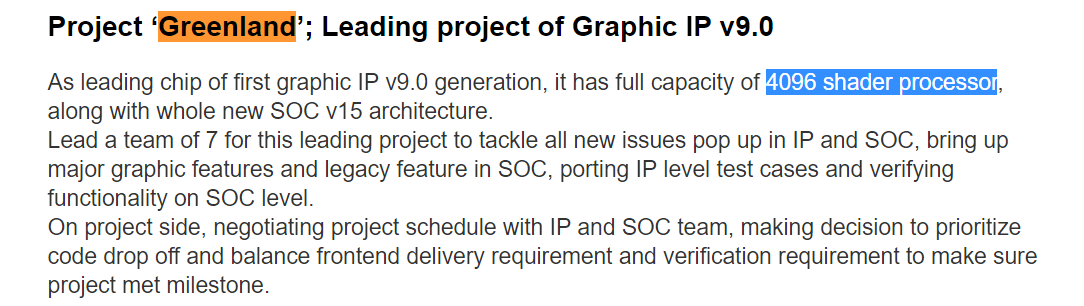
AMD’s upcoming flagship GPU could feature 4096 Stream Processors, as revealed by AMD’s employee via LikedIn profile.
AMD Greenland / Vega 10 — 4096 Stream Processors confirmed?
Guys over at 3DCenter discovered a very interesting piece of information. According to Yu Zheng LikenIn profile, who is a research and development manager at AMD, company has been working on new flagship graphics processing unit also known as Greenland or Vega 10.
The profile reveals that Greenland is the leading project of Graphic IP v9.0. In other words, this is the new flagship GPU that will succeed the most powerful Fiji processor currently offered by AMD.
The graphic IP level 9.0 most likely stands for Vega architecture (the first to feature HBM2 memory). The project is tied with AMD’s SoC (System on a Chip) v15 architecture, which could suggest that future AMD APUs could also be somewhat connected to Polaris and Vega GPUs.
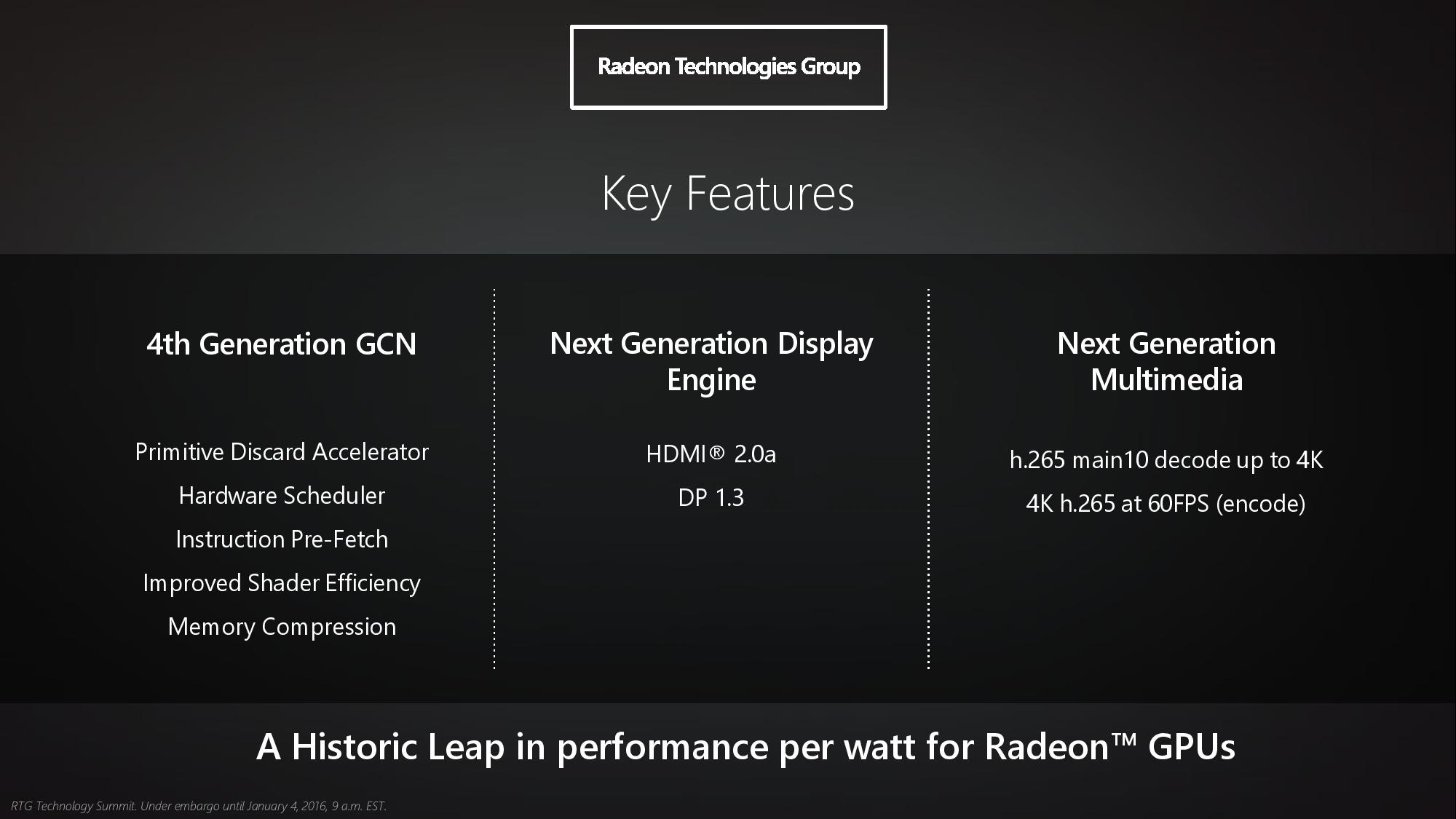
If Greenland indeed features 4096 Stream Processors, it would therefore be exactly the same as Fiji. The upgrade to 14nm FinFET architecture would surely improve power efficiency. However would it also boost the performance per stream processor? Well, according to official slides yes, as AMD promised Graphics Core Next 4.0 will improve shader efficiency.
Also don’t forget that Stream Processors are not the only major processing units in GPU. AMD could also adjust the number of Raster Engines to 128, that would surely improve performance.
Here’s an updated chart comparing all known Polaris and Vega GPUs.
| AMD Vega & Polaris GPUs (To Be Confirmed) | ||||
|---|---|---|---|---|
| March 26th 2016 | AMD R9 490? | AMD Fury X2 | AMD R9 470? | AMD R7 460? |
| GPU | Vega 10 / Greenland | Fiji | Polaris 10 / Ellesmere | Polaris 11 / Baffin |
| Fabrication Process | 14nm FinFET | 28nm | 14nm FinFET | 14nm FinFET |
| Compute Units | 64 | 64 | 36 | ? |
| Stream Processors | 4096 | 4096 | 2560-2304 | ? |
| TMUs | ? | 256 | ? | ? |
| ROPs | ? | 64 | ? | ? |
| Computing Power | ? | 8.6 TFLOPS | ~3.7 TFLOPs | ? |
| Core clock | ? | 1050 MHz | ~800 MHz | ~1000 MHz |
| Memory Clock | 1000 MHz | 500 MHz | ~1500 MHz (6 GHz) | ~1750 MHz (7 GHz) |
| Memory Bus | 4096-bit | 4096-bit | 256-bit | 128-bit |
| Memory | 8GB HBM2 | 4GB HBM1 | 8GB GDDR5 | 4GB GDDR5 |
| Bandwidth | ~1024 GB/s | 512 GB/s | 192 GB/s | 112 GB/s |
| Launch Date | 2016/2017 | June 2015 | Q3 2016 | Q3 2016 |